⚛️ Diving into the World of Semiconductors: From Atoms to Crystals
Semiconductors play a crucial role in modern electronics, bridging the gap between conductors and insulators.
Understanding their unique properties is essential to grasp how everyday devices like diodes and transistors function.
🟠 In this article, we’ll explore the fundamental concepts of semiconductors, from atomic structure to crystal formation, and explain how doping transforms their electrical behavior.
Conductor
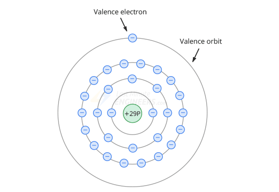
- The nucleus of a copper atom has 29 protons(+) (positive charge).
- There are 29 electrons(-) revolving around the nucleus (negative charge).
In electronics, only the last orbit is important - the valence orbit - it determines the conductivity of the atom.
Net Charge
To determine the total charge of an atom, it is necessary to subtract all electrons (except the last/valence orbit) from the charge of the nucleus.
Example for copper = +1 (+29 protons - 28 electrons)
Free Electrons
Since the total charge of the nucleus is +1 (after subtraction), the attraction between the nucleus and the valence electron (in the last orbit) is very weak.
Even nominal voltage can easily knock this electron out of the copper atom and make it flow through the material.
That is why the valence electron is called a free electron.
And the flow of these free electrons is called Current
* the conductivity of an atom depends on the number of valence electrons.
* 1 valence electron - best conductor
* 8 valence electrons - best insulator
Insulators
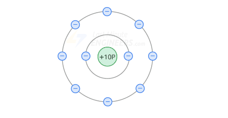
The atomic structure of neon is a good insulator.
The net charge of the nucleus is +8, so the external attraction felt by the valence electrons is very large.
Therefore, due to the lack of free electrons, insulators do not conduct current.
If a high enough voltage is applied to an insulator, the force will be so great that the valence electrons will literally be torn from their atoms. This will cause conduction. In air, you will see this as an arc or flash. In solid materials, the heat generated will char the material.
Semiconductors
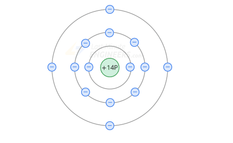
A semiconductor is an element that is neither a good conductor nor a good insulator.
The best semiconductors have 4 valence electrons.
Atomic structure of silicon - an example of a semiconductor.
There are 4 electrons in the valence orbit, so the net charge of the silicon nucleus is +4
Since the number of valence electrons of silicon is 4, this makes it in the middle of a conductor and an insulator - semiconductor
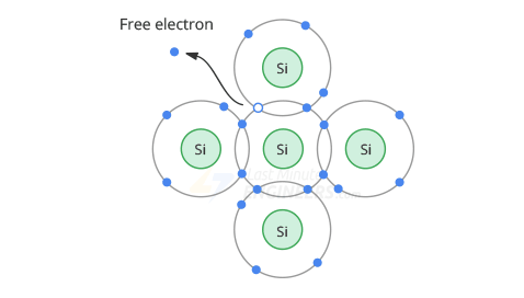
Silicon crystals

When silicon atoms combine to form a crystal, they arrange themselves into a systematic structure
In this case, each silicon atom begins to share its valence electrons with the 4 valence orbits of the neighboring 4 atoms.
Each atom now has 8 electrons in its orbit (4 of its own + 4 (1 from each neighbor))
Covalent Bonds
Because of the sharing, the valence electrons are now not owned by any one atom
These shared valence electrons are attracted by neighboring atoms with equal and opposite forces, causing them to form a connection.
The following figure illustrates the concept of covalent bonds, with each straight line representing one shared electron.
{{ img(src = "/images/basic electronics/covalent_bonds.png) }}
This opposite attraction holds the silicon atoms together and gives them strength.
Holes
At room temperature, the thermal energy in the air causes the atoms in a silicon crystal to vibrate.
These vibrations remove an electron from its valence orbit, causing it to float freely throughout the crystal.
The loss of an electron creates a vacancy in the valence orbit called a Hole
This hole acts as a positive charge, since the loss of an electron produces a positive ion.
When a free electron comes close to a hole, it is attracted to it and falls into it.
The process of merging a free electron and a hole is called Recombination.
Flow of free electrons and holes
If you connect a battery across a clean silicon crystal, the thermal energy will produce a free electron and a hole.
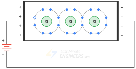
The applied voltage causes the free electrons to move to the left and the holes to the right.
When the free electrons reach the left end of the crystal, they enter the outer wire and flow toward the positive terminal of the battery.
- On the other hand, free electrons at the negative terminal of the battery flow to the right end of the crystal.
- They enter the crystal and recombine with the holes that have reached the right end of the crystal.
- Thus, a constant flow of free electrons and holes is established inside the semiconductor.
- Free electrons and holes are often called carriers because they carry charge from one place to another.
Doping a Semiconductor
In a pure silicon crystal, each atom uses 4 valence electrons to connect with the valence orbits of neighboring atoms.
This reduces the number of electrons available for conduction, so the crystal acts as an insulator.
To increase the number of holes and, therefore, free electrons, thereby increasing the conductivity of the crystal, it must be doped.
Doping is the process of adding impurities to a pure silicon crystal to change its electrical conductivity.
The more dopant added, the more free electrons and holes there are, which leads to an increase in conductivity.
This means that a lightly sealed semiconductor has a high resistance, while a heavily doped semiconductor has a low resistance.
How is silicon crystal doped? First, pure silicon crystal is melted. This breaks the covalent bonds and turns the silicon from a solid to a liquid state. To increase the number of free electrons, pentavalent atoms are added to the molten silicon. And to increase the number of holes, tritant atoms are added. After it cools, it turns into a solid crystalline structure.
n-type semiconductor
Silicon doped to increase the number of free electrons is called an n-type semiconductor (n- means negative)
pentavalent impurities (phosphorus, antimony, arsenic) are added to silicon. To increase the number of free electrons.
Phosphorus atom diagram-
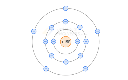
In an n-type semiconductor, the pentavalent atom is in the middle, and 4 silicon atoms surround it.
A 5-valence orbital can hold no more than 8 electrons.
When the valence orbits intersect, the silicon atoms share 1 electron with the phosphorus orbital, thereby releasing 1 free electron from the phosphorus valence orbital
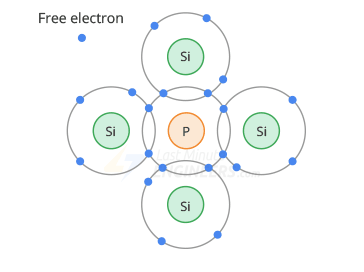
Each 5-valence atom in a silicon crystal releases 1 free electron, such impurities are called donor impurities
In an n-semiconductor, there are more free electrons than holes, so free electrons are called major carriers, and holes minor.
p-type semiconductor
Silicon doped to increase the number of holes is called a p-type conductor (p- means positive)
For this, 3-valent impurities (aluminum, boron, gallium) are added
Boron atom diagram -
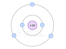
In a p-type doped crystal, the 3-valent atom is in the middle, on its valence orbit there will be only 7 electrons (3 of its own + 1 from each silicon atom).
Consequently, on the valence orbit of each 3-valent atom there appears a hole.
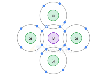
In these types of semiconductors, holes are now called majority carriers, and electrons are called minor.
A 3-valent atom is also called an acceptor atom, since each hole it contributes can accept a free electron during recombination.
Image Source: LME