⚛️ The Aesthetics of Semiconductor Destruction: Understanding the PN Junction
The PN junction is the fundamental building block of many semiconductor devices, from diodes to transistors and solar cells.
Understanding how this tiny boundary between p-type and n-type materials controls the flow of electrical current is key to grasping modern electronics.
🟠 In this article, we’ll explore the structure, behavior, and biasing conditions of the PN junction — revealing the delicate balance that makes semiconductor devices work.
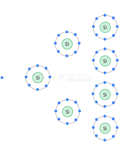
The PN Junction
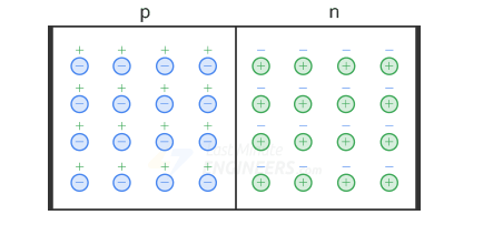
- for positive - the nucleus of each 3-valent atom produces one hole (+)
- for negative - the nucleus of each 5-valent atom creates one free electron (-)
When a silicon crystal is created with a p-type material on one side and an n-type material on the other side - the boundary between them is called a PN junction
A PN crystal is called a junction diode. The word diode is an abbreviation for two (di) electrodes
There are 3 possible bias conditions for a PN junction:
- Equilibrium or Zero Bias - no external voltage is applied to the PN junction.
- Reverse Bias - when the
positivesource terminal is connected to the n-type, and thenegativesource terminal is connected to the p-type - Forward Bias - the
negativesource terminal is connected to the n-type, and thepositiveterminal is connected to the p-type
Equilibrium (zero bias)
Without external influence, balance is achieved.
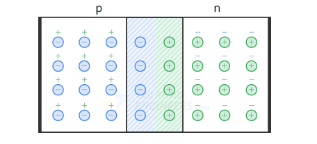
The Depletion Region
Because of the high concentration, the electrons in N repel each other and spread (diffuse) into the P region.
In the P region, this free electron coming from N - fills a hole.
Thus, each time an electron crosses the junction and recombines with a hole, it creates a pair of ions.
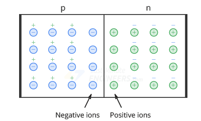
Each pair of negative and positive ions at the boundary is called a diopole When a diopole is created, the majority carriers on each side are extracted from the atom, so this zone is called a depletion region.
Barrier Potential
Each region (diopole) has an electric field between the positive and negative ions.
Whenever a free electron from P tries to enter the depletion region, the electric field pushes it back into the N region.
The strength of the electric field increases with each recombination of holes and electrons inside the depletion region.
- Therefore, the electric field eventually stops diffusion and equilibrium occurs
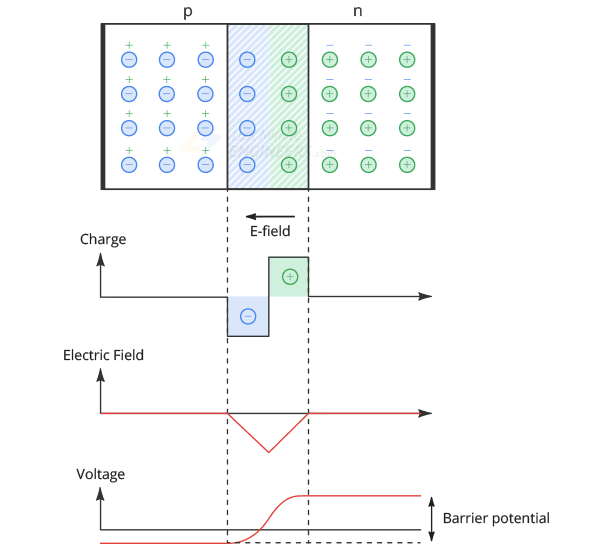
The electric field between the ions is equivalent to a potential difference called the barrier potential.
At room temperature, the barrier potential is approximately 0.3V for germanium diodes and 0.7V for silicon diodes.
Forward Bias
p-type is connected to the positive side of the source and the n-type to the negative side.
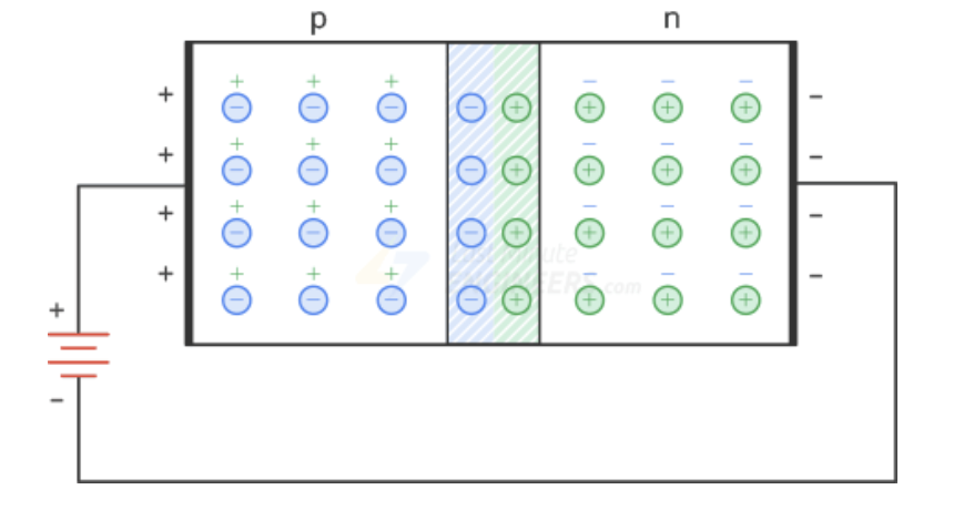
With this connection, the holes in the P and the free electrons in the N are pushed toward the junction
If the battery voltage is less than the barrier potential (0.7V), the free electrons have enough energy to pass through the depletion layer and recombine with the holes.
- Thus, the depletion region shrinks.
When a free electron recombines with a hole, it becomes a valence electron. As a valence electron, it continues to move to the left, passing from one hole to another, until it reaches the left end of the diode.
When it leaves the left end of the diode, a hole is formed at that location and the process repeats.
Since billions of electrons are flowing at the same time, a continuous current is obtained.
Reverse Bias
p-type is connected to the negativeside of the source and the n-type to positive side.
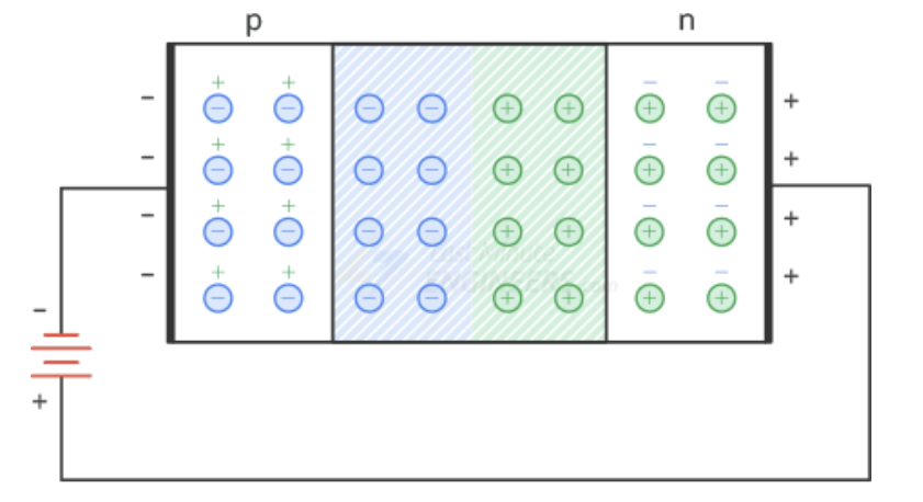
The negative terminals of the battery attract holes, and the positive terminals attract free electrons.
This causes the free electrons to flow away from the junction, leaving positive and negative ions behind.
- Thus, the depletion region increases.
The width of the depletion region is proportional to the reverse voltage.
The depletion region stops growing when its potential difference becomes equal to the applied reverse voltage.
Reverse Current
The reverse current in a diode consists of the minority carrier current and the surface leakage current.
This reverse current is so small that it is considered to be almost zero.
Surface-Leakage Current
In a reverse biased diode, there is another current.
A small current flows along the surface of the crystal, known as the surface leakage current.
The atoms on the top and bottom surfaces of the crystal have no neighbors, they have only 6 electrons in the valence orbit.
This means that each surface atom has 2 holes.
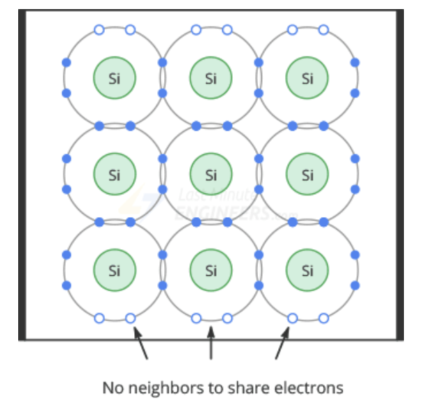
This causes electrons to move through the surface holes from the negative pole of the battery to the positive pole of the battery.
Thus, a small reverse current flows along the surface.
Breakdown
There is a limit to how much reverse voltage a diode can withstand before it reaches breakdown voltage and fails.
Once the breakdown voltage is reached, a large number of minority charge carriers are formed in the depletion region due to the avalanche effect and the diode begins to conduct current in the reverse direction.
Avalanche Effect
When the reverse voltage increases, it causes the minority carriers to move faster.
These minority carriers begin to move at a tremendous speed, colliding with the crystal atoms, knocking out valence electrons from them, creating more free electrons.
The number of free electrons increases in geometric progression 1, 2, 4, 8, 16....
This produces a significant reverse current in the diode and continues until the reverse current becomes large enough to destroy the diode.
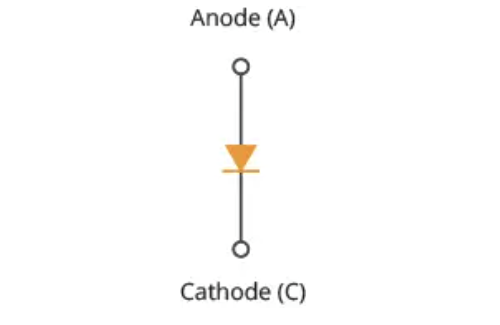
Diode Schematic Symbol
An arrow pointing from the p-side to the n-side.
The p-side is called the anode and the n-side is called the cathode.
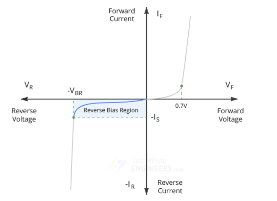
Diode I-V Characteristics
A basic diode circuit in which the diode is forward biased.
A series resistor RS is typically used to limit the magnitude of the forward current IF .
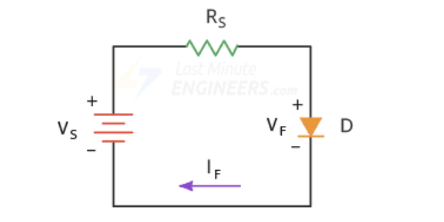
After connecting this circuit, if you measure the voltage and current of the diode for forward and reverse bias, and plot it, you will get a graph that looks like this:
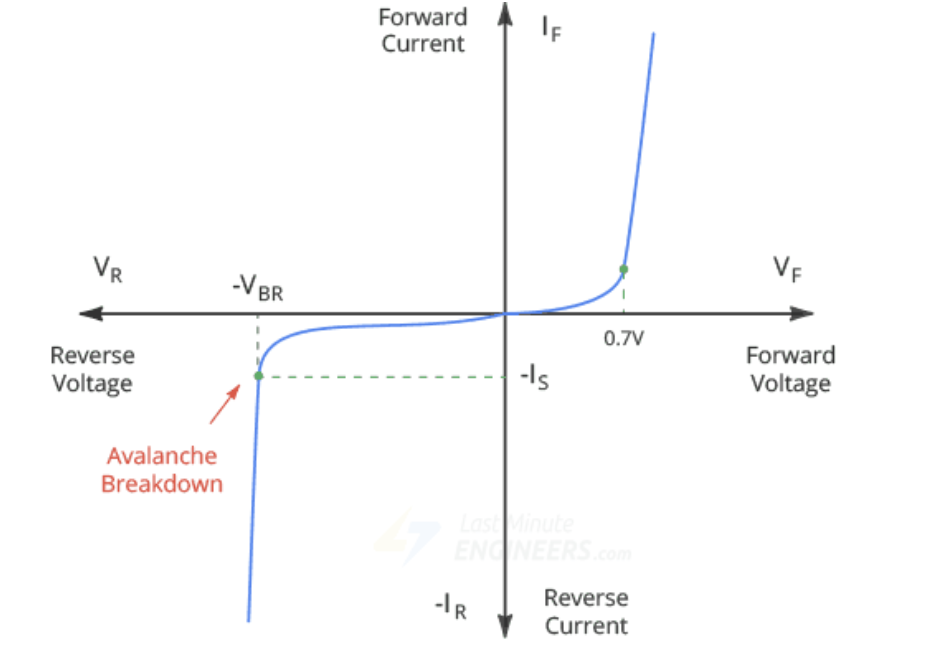
This plot is called Current-Voltage (I-V) characteristics.
This is the most important diode characteristic because it defines how much current flows through the diode for a given voltage.
A resistor is a linear device, its I-V characteristic is a straight line.
A diode's IV characteristic is a curve - this is due to the barrier potential.
Depending on the voltage applied to it, it will operate in one of 3 areas:
- forward bias
- reverse bias
- breakdown
Forward Bias Region
When the diode voltage is less than the barrier potential, a small current flows through the diode.
When the diode voltage exceeds the barrier potential, the current flowing through the barrier increases rapidly.
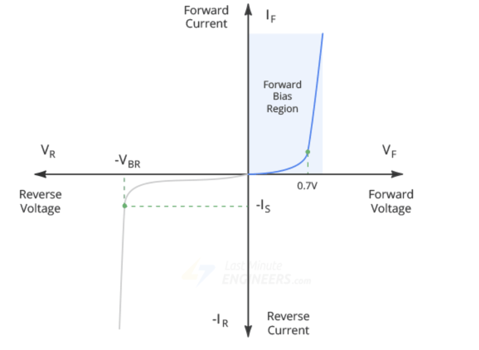
The voltage at which the current begins to increase rapidly is called the forward voltage (VF) of the diode.
It is also called cut-in voltage or knee voltage.
Reverse Bias Region
The reverse bias region exists between zero current and breakdown.
In this region, a small reverse current flows through the diode.
Breakdown Region
If we continue to increase the reverse voltage, then eventually a breakdown state will be reached.
At this point, an avalanche breakdown occurs in the depleted layer of the semiconductor and the diode begins to actively break through the current in the reverse direction, which leads to its destruction.
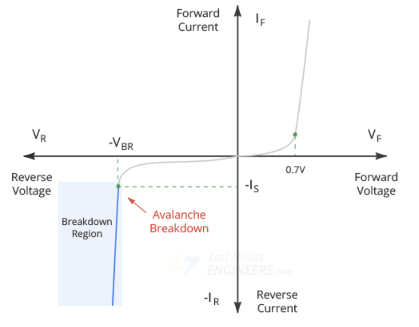
Image Source: LME